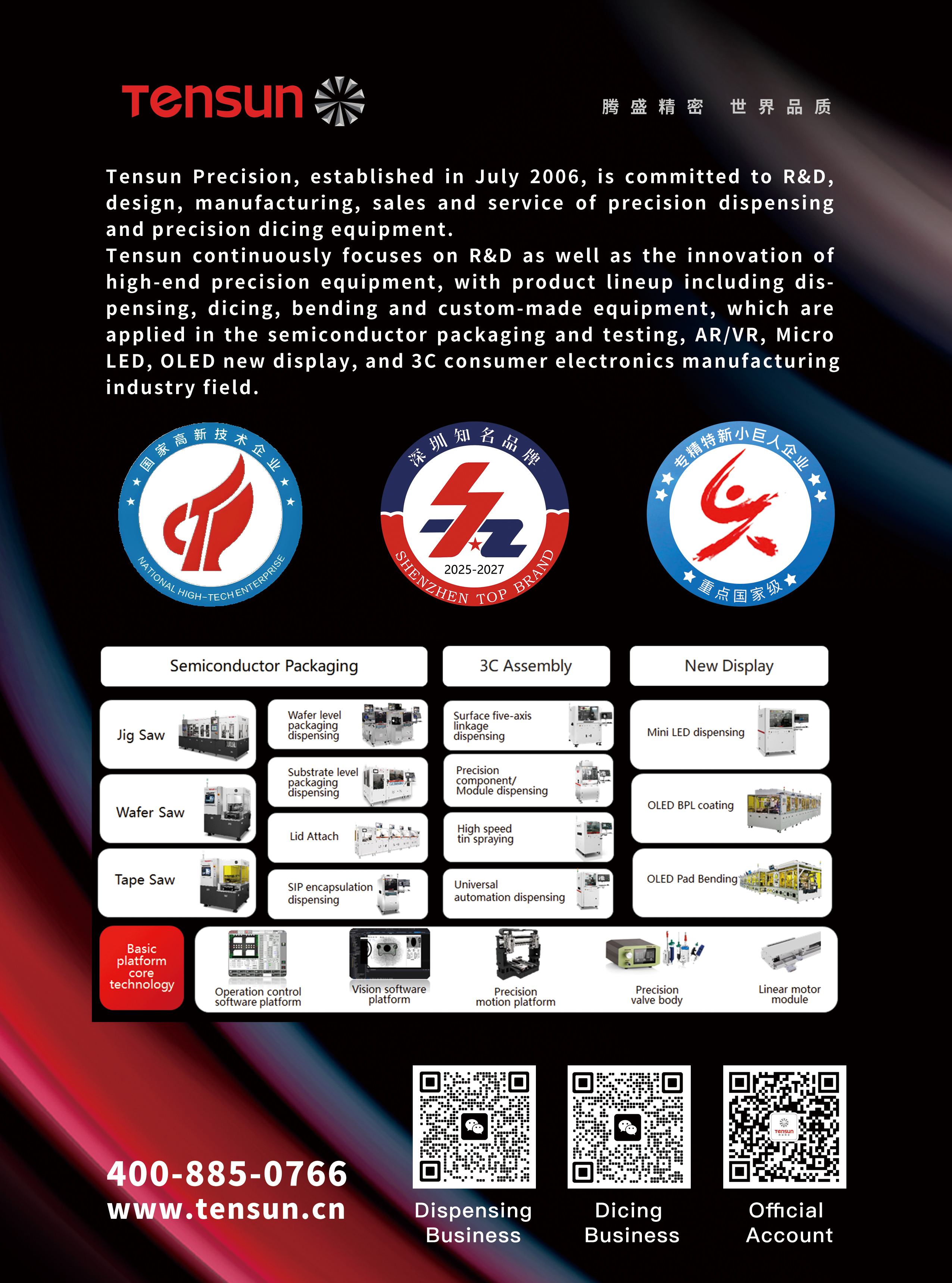

Advanced Packaging Grows Rapidly, Tensun Expands in Semiconductor Testing and Packaging
Time:2025-05-19 16:46:38 Browse:173 Editor:Tensun Precision
Preface
The US announced the National Advanced Packaging Manufacturing Program, prioritizing materials and substrates for investment. As a key way to extend Moore's Law, advanced packaging is of great importance. With policy changes, the packaging capacity ratio at home and abroad will change. It's a chance as well as a challenge for everyone to fight for the dominant right.
Overseas Packaging Giants Enter the US
Recently, the US announced the first R&D investment project under the CHIPS and Science Act, allocating around $3 billion to fund the US chip packaging industry (NAPMP). The six priority investment areas are: 1) packaging materials and substrates, 2) equipment, processes, and tools, 3) power delivery and thermal management for advanced packaging components, 4) optical communications and connectors, 5) Chiplet ecosystem, and 6) co-design of multi-Chiplet systems and automated tools.
In the global advanced chip packaging capacity, China accounts for about 38%, while the US only accounts for 3%. As of February, the US government has received over 460 incentive applications for US semiconductor manufacturing and related projects. Among them, foreign companies plan to establish packaging projects in the US, such as SK Hynix's $15 billion investment to build advanced packaging facilities in the US, Amkor's plan to establish an advanced packaging and testing factory, and TSMC's ongoing negotiations. The entry of overseas packaging giants into the US may increase its share in the advanced packaging field and highlights the importance of advanced packaging in the post-Moore era.
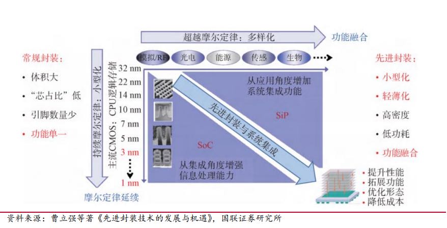
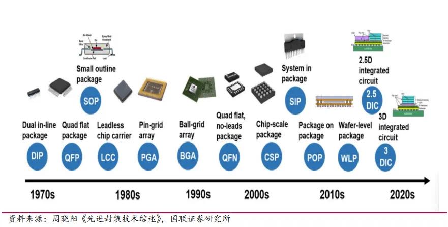
As per the International Technology Roadmap for Semiconductors (ITRS), future chip-tech development will primarily focus on two aspects: one is shrinking transistor feature sizes in line with Moore's Law; the other is expanding Moore's Law via advanced packaging tech for diverse-type development.
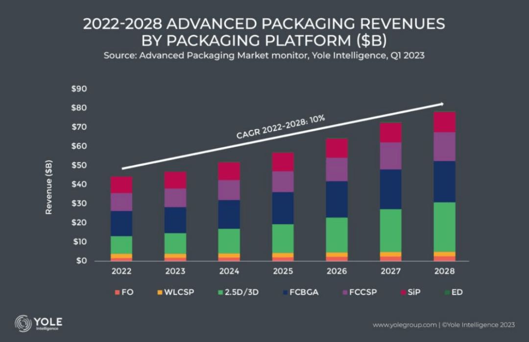
According to Yole's forecast, the global advanced packaging market will expand from $44.3 billion in 2022 to $78.6 billion by 2028, registering a CAGR of 10.6%. Within this market, 2.5D/3D packaging is the fastest-growing segment, with a CAGR of 14.34% from 2021 to 2027. This growth is mainly driven by applications like AI, HPC, and HBM.
Large Models Demand Massive Computing Power, with Advanced Packaging Technology as the Key
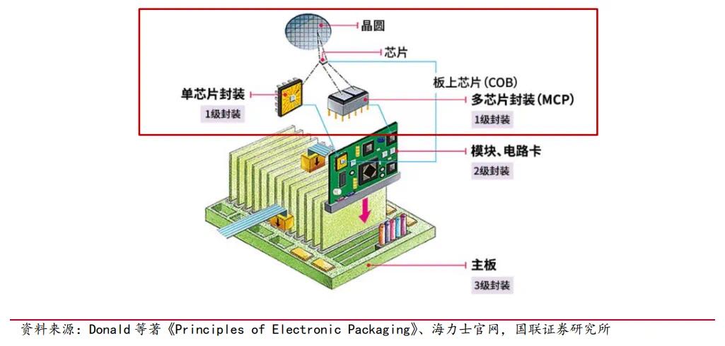
Semiconductor packaging once only covered wafer cutting and chip packaging. But to meet the rising need for high-performance chips, it's now moving towards miniaturization, high reliability, stacking, and high-speed signal transmission, advancing to advanced packaging.
In the AI age, computing power is crucial. Chiplet technology is key for high-end computing chips, with advanced packaging being vital for Chiplet implementation. Thus, developing advanced packaging is crucial globally.TSMC, Intel, Samsung, and SK Hynix are key players in advanced packaging tech like HBM and Chiplet.
TSMC's 3DFabric includes 2.5D CoWoS and 3D SoIC. CoWoS, at Generation 5, stacks chips on a silicon interposer for interconnection. SoIC, leveraging CoWoS and WoW, is a cutting-edge 3D packaging tech. Major chipmakers like NVIDIA, Apple, AMD, Broadcom, and Marvell have adopted these technologies.
Intel's Advanced Packaging Technologies: 2.5D EMIB and 3D Foveros, Co-EMIB, and Hybrid Bonding.
Intel's 2.5D EMIB uses an ultra-fine bump pitch to achieve high interconnect density, offering higher bandwidth and lower power consumption than organic substrate-based methods; Foveros, Co-EMIB, and Hybrid Bonding are advanced 3D packaging technologies. They may replace ABF substrates with glass substrates to enhance signal speed and power efficiency.
Samsung's Advanced Packaging Technologies: 2.5D I-Cube, FO-PLP, and 3D X-Cube, SAINT.
Samsung's 2.5D I-Cube integrates logic and memory chips on an interposer, rivaling TSMC's CoWoS in capability; 3D X-Cube uses TSV to stack memory on logic chips, shortening interconnects to cut power use and boost speed.
SK Hynix's Advanced Packaging Technology**: 2.5D Fan-Out Packaging for DRAM.
Its 2.5D Fan-Out technology places two DRAM chips side-by-side, combining them into one. This slims the chip as no substrate is added beneath.
In China, JCET focuses on system-level, wafer-level, and 2.5D/3D packaging. TFME has a strategic focus on multi-chip modules, integrated fan-out, and 2.5D/3D packaging. HTT has mastered SiP, FC, TSV, Bumping, Fan-Out, WLP, and 3D packaging. Yongxi Electronics specializes in FCCSP, FCBGA, FC, SIP, BGA, QFN, and MEMS packaging.
Compared to the global market, China's advanced packaging layout still needs optimization.
Tensun Intensifies Equipment Layout in Semiconductor Packaging
In advanced packaging, precision demands on processes and equipment exceed those of traditional packaging. For instance, backside thinning requires flatter warpage, and wafer cutting needs higher speed and accuracy. However, the domestication rate of packaging equipment in China has risen slowly in recent years, with low domestic rates for wire bonders, pick-and-place machines, and dicing saws, leaving substantial import - substitution potential.
Tensun has been expanding in the pan-semiconductor cutting field since 2014. Its 2015 SDS and ADS cutting equipment, suitable for wafer/QFN/GBA/LGA/LED packaging/SIP products, has seen over 1,000 12 - inch Tape Saw units sold. In 2020, Tensun initiated Jig Saw development, achieving mass production and shipment after two years. This multi-functional equipment, integrating cutting and sorting, serves mainstream packaging products like QFN, BGA, LGA, and DFN, enabling import substitution for domestic packaging firms.
This year, Tensun launched several new dispensing systems for advanced semiconductor packaging. These include ultra-precision wafer-level packaging dispensing equipment compatible with 8-to 12-inch wafers, for wafer-level underfill and coating processes. Also, there's underfill equipment for FC-BGA, FC-CSP, and SIP packaging, featuring an optional tilting dispensing system that can achieve a KOZ as narrow as 200μm.