
Wafer-level Packaging Tech Drives Semiconductor Industry Growth
Time:2025-05-13 16:05:40 Browse:42 Editor:Tensun Precision
Preface
Per recent data from IDC and the MIIT, as of Feb 2024, shipment in emerging fields like smartphones and new energy vehicles has risen, boosting global semiconductor industry growth. The semiconductor
packaging and testing sector is still moving towards miniaturization, integration, and low-power consumption. Advanced packaging forms like wafer-level packaging tech are becoming industry trends.
Recovery of 3C & Auto Industries Spurs Significant Growth in Semiconductor Sector
According to Counterpoint Research’s “Smartphone 360 Report”, global smartphone shipments hit a decade-low in 2023, and in Q4 they merely matched the previous year’s level. In Q1 2024, with the phone replacement cycle underway, AI smartphone demand shows slight growth. Emerging markets like India, the Middle East, and Africa are driving iPhone sales, while Huawei keeps growing in China’s high-end smartphone market.
The PC market, after years of slump, has nearly returned to pre-pandemic shipment levels. Some analysts believe that the tech update from AI-chip-embedded PCs and the replacement cycle will accelerate PC market growth in 2024. Recently, PC brands have been focusing on AI PCs. For example, Lenovo leading the PC market launched six new AI PC products at a time; Apple released the AI PC MacBook Air; Honor presented the AI PC MagicBook Pro 16; Huawei introduced the MateBook X Pro based on its Pangu AI.
The automotive market is experiencing significant growth with the rise of electrification. Intelligent vehicles are moving towards modularity and centralization. Car manufacturers' price cuts and subsidies, along with new model launches, are boosting the industry. Xiaomi's SU7 stands out for its attractive pricing compared to rivals like the Tesla Model 3, Zeekr 001, and BYD Han EV.
The recovery of the 3C and automotive industries highlights AI's growing influence. AI demands higher storage capacity and performance. High-end smartphones are now mostly in the 512GB to 1TB range, with the average phone storage expected to exceed 200GB this year. Unlike traditional PCs, AI PCs feature a "CPU + GPU + NPU" architecture, supporting local AI models. This requires faster data transfer speeds and larger storage capacity. Similarly, Level 3 and above autonomous vehicles will soon enter the TB era for per-vehicle storage.
Driven by AI-powered cloud computing and the product cycle renewal of terminal devices, the global semiconductor industry is on an upward trajectory, with sales growing and a recovery in the industrial cycle imminent. In February, global semiconductor sales reached $46.17 billion, up 16.3% year-on-year, marking the fourth straight month of positive growth, per SIA. China's semiconductor sales stood at $14.13 billion, surging 28.8%, the highest growth rate globally.
Wafer-level packaging is gaining traction.
Amid the AI boom and downstream market recovery, the semiconductor industry is growing rapidly. As Moore's Law nears its physical limits, front - end and back - end processes are converging. Advanced packaging, which offers efficiency, cost-effectiveness, and performance, is a key focus and will reshape the industry's competitive landscape.
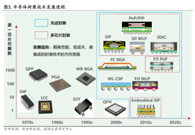
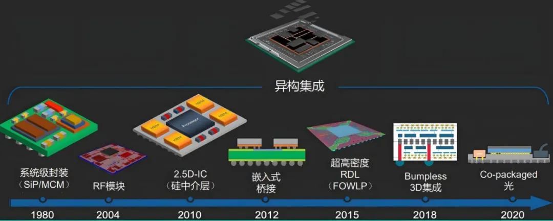
So far, development of semiconductor packaging technology has experienced four stages roughly:
(1) Before the 1980s, component insertion dominated, mainly featuring through-hole packaging (DIP).
(2) Mid-1980s, surface mount technology emerged, led by small outline packaging (SOP).
(3) 1990s, area array packaging became mainstream, including ball grid array (BGA), chip scale packaging (CSP), and flip chip.
(4) Since 2000, advanced packaging technologies like wafer-level packaging (WLP), through-silicon via (TSV), 2.5D, 3D packaging, and system-in-package (SiP) have developed.
Advanced packaging is advancing towards miniaturization, thinness, fine pitch, and high integration. Its future focuses on wafer-level and system-in-package technologies.
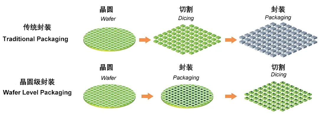
Wafer-level packaging (WLP) involves encapsulating an entire wafer before dicing it into individual chips.
System-in-package (SiP) integrates multiple functional chips (e.g., processors, memory) into a single package to achieve a complete functionality.
Per Yole, the global advanced packaging market will grow from $44.3 billion in 2022 to $78.6 billion in 2028, at a 10.6% CAGR, driving growth in the packaging and testing sector.
Tensun Wafer-level Packaging Solutions
Advanced packaging is developing rapidly, with TSMC's CoWoS being the most representative. CoWoS includes:
- CoWoS-S: Uses silicon interposers for chip interconnection.
- CoWoS-R: Employs redistribution layers for interconnection.
-CoWoS-L Combines the technologies of CoWoS-S and CoWoS-R.
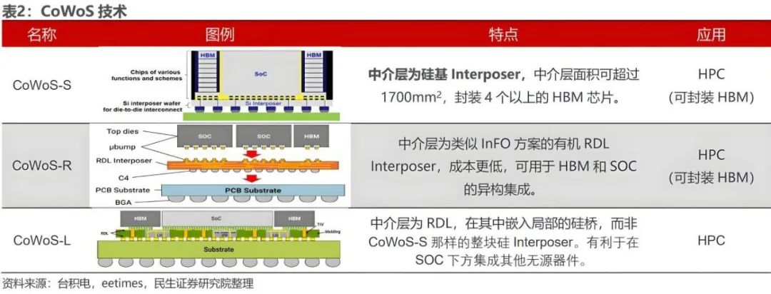
In CoWoS packaging, chips are first connected to a wafer or RDL via flip-chip technology, then linked to a substrate to form CoWoS. In the Chip on Wafer process, Underfill dispensing is required. Unlike substrate dispensing, it's done before wafer dicing, demanding a specialized wafer-level dispensing system.
The WDS2500 wafer-level dispensing system, developed by Tensun for wafer-level Underfill processes, features a high-speed, high-precision, and stable dispensing platform. Equipped with a dedicated EFEM module for automatic material handling, it adopts a 1-to-2 configuration, integrating two high-precision dispensers into a fully automated system. The system meets semiconductor industry standards for cleanroom environments, ESD control, and SECS/GEM communication protocols.
To meet the stringent wafer-level Underfill dispensing requirements, the system adopts four thermal-control strategies:
Piezoelectric module temperature monitoring and compensation stabilize the crash needle displacement.
The glue tube thermostat keeps adhesive properties stable.
Nozzle and manifold heating ensures smooth adhesive flow.
A heater on the valve-standby platform maintains ambient temperature for
The wafer-handling unit consists of three standard core components from an industry - leading brand and two platforms. It handles 8-to 12-inch wafers and transparent / semi - transparent glass. The heating platform has a surface temperature variation of ±3℃. The lift mechanism uses servo motor control for stepless speed adjustment, ensuring smooth and reliable operation.